


Introduction to the Company:
Cadence is extending its semiconductor technology knowledge into the system-level design and fueling artificial intelligence with our Intelligent System Design™ strategy.
This means they can offer the world’s most creative companies the broadest, most integrated end-to-end solution to help today’s electronic designers do their best work creating tomorrow’s products.
They work with the world’s most innovative companies developing solutions for applications in artificial intelligence, 5G, autonomous driving, and industrial IoT devices. With Cadence technology, expertise, and collaboration, its customers turn great ideas into reality faster.
How To create a library and build a schematic of an Inverter
Below steps explain the creation of the new library “myDesignLib” and we will use the same throughout this course for building various cells that we going to create in the next labs. Execute Tools – Library Manager in the CIW or Virtuoso window to open Library Manager.
Creating a New library:
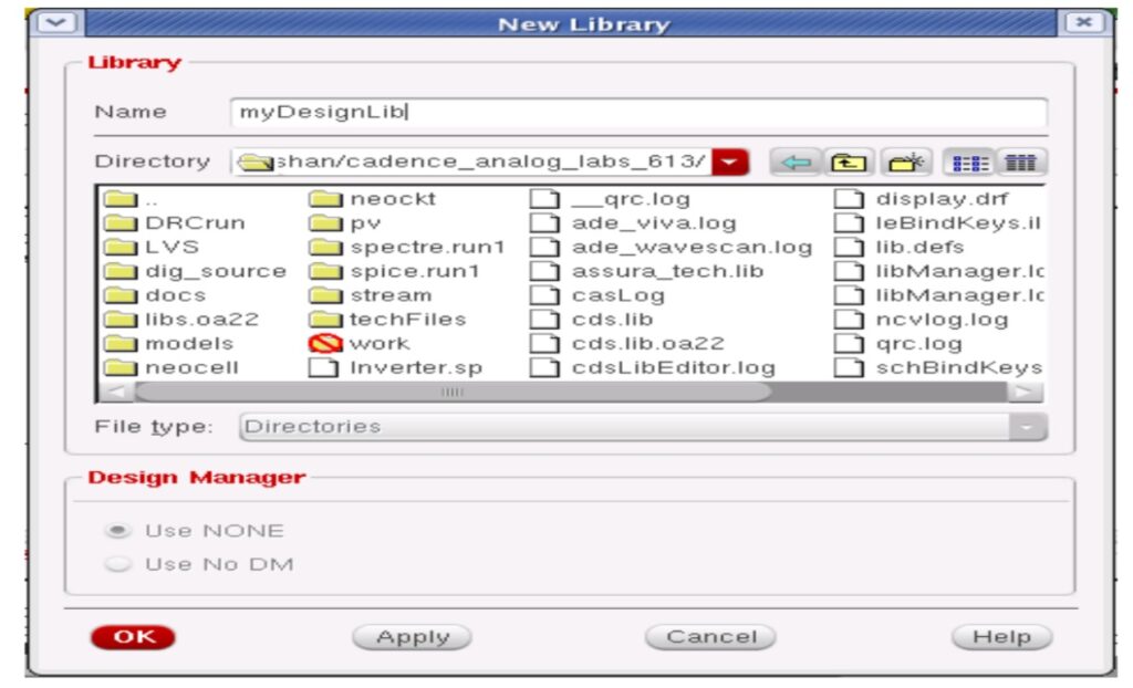
- In the Library Manager, execute File – New – Library. The new library form appears.
- In the “New Library” form, type “myDesignLib” in the Name section.
- In the field of Directory section, verify that the path to the library is set to /home/student/Desktop/myDesign and click OK.
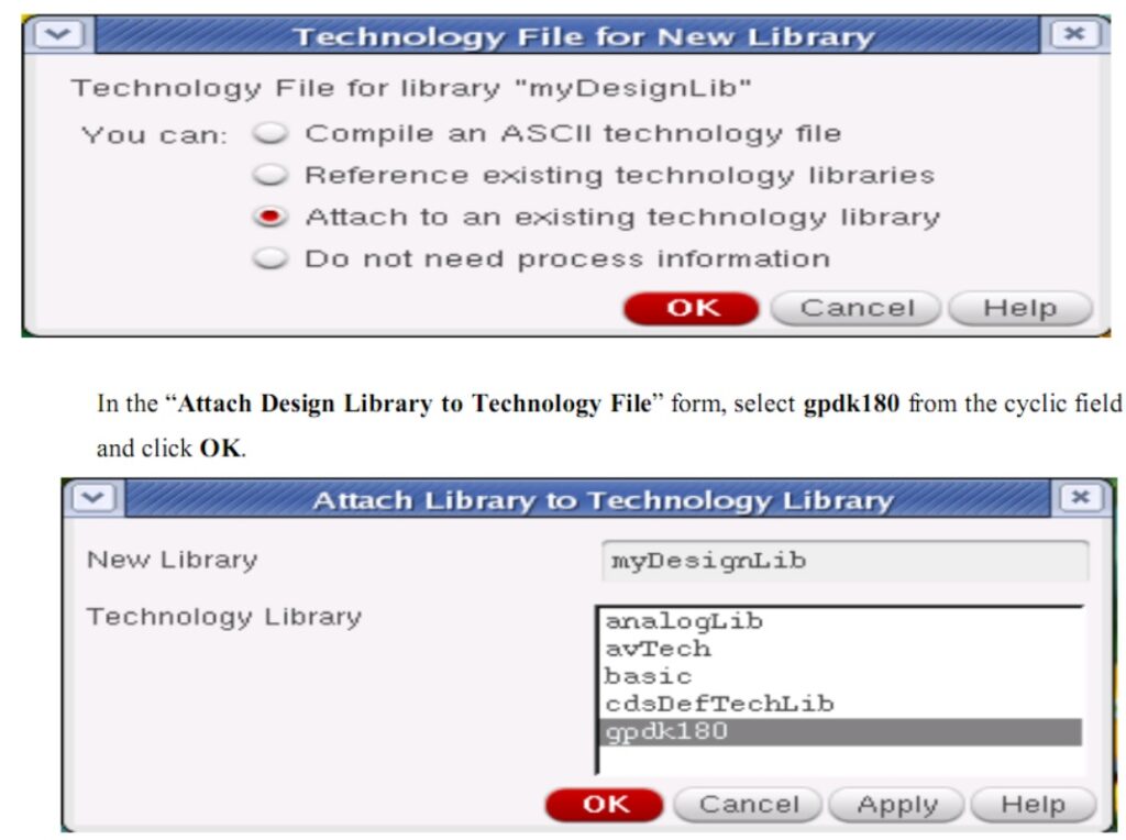
- Note: A technology file is not required if you are not interested to do the layouts for the design.
- In the next “Technology File for New library” form, select option Attach to an existing techfileand click OK.
- After creating a new library you can verify it from the library manager.
- If you right-click on the “myDesignLib” and select properties, you will find that gpdk180 library is attached as techlib to “myDesignLib”.
Creating a Schematic Cellview:
In this section, we will learn how to open a new schematic window in the new “myDesignLib” library and build the inverter schematic as shown in the figure at the start of this lab.
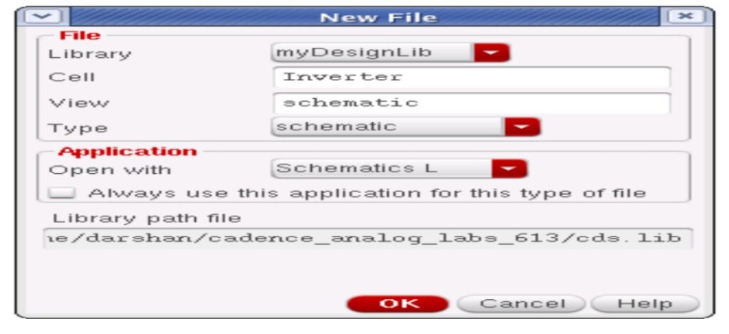
- In the CIW or Library manager, execute File – New – Cellview.
- Set up the New file form as follows:
- Do not edit the Library path file and the one above might be different from the path shown in your form.
- Click OK when done the above settings. A blank schematic window for the Inverter design appears.
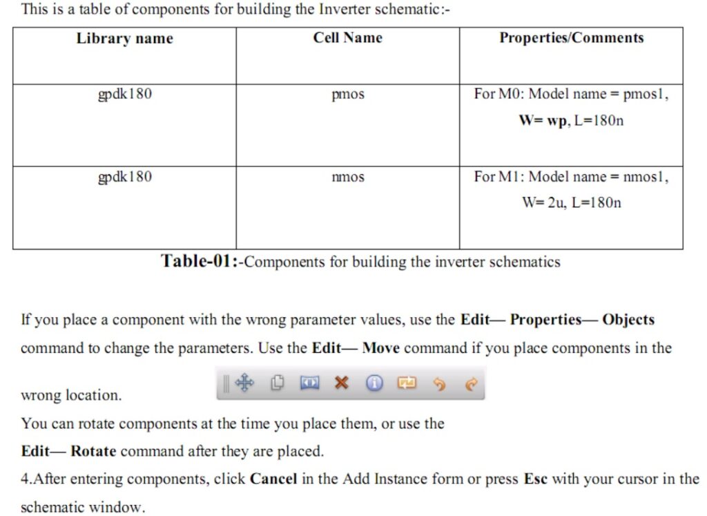
Adding Components to the schematic:

- In the Inverter schematic window, click the Instance fixed menu icon to display the Add Instance form. Tip: You can also execute Create — Instance or press i.
- Click on the Browse button. This opens up a Library browser from which you can select components and the symbol view. You will update the Library Name, Cell Name, and the property values given in the table on the next page as you place each component.
- After you complete the Add Instance form, move your cursor to the schematic window and click left to place a component.
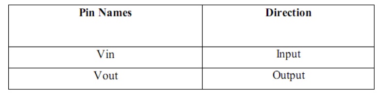
Adding pins to Schematic:
- Click the Pin fixed menu icon in the schematic window.
- You can also execute Create — Pin or press p.
- The Add pin form appears.
- Type the following in the Add pin form in the exact order leaving space between the pin names.
- Make sure that the direction field is set to input/output/input-output when placing the input/output/input pins respectively and the Usage field is set to the schematic.
- Select Cancel from the Add – pin form after placing the pins. In the schematic window, execute Window— Fit or press the f bindkey.
Adding Wires to a Schematic:
Add wires to connect components and pins in the design.
- Click the Wire (narrow) icon in the schematic window. You can also press the w key, or execute Create — Wire (narrow).
- In the schematic window, click on a pin of one of your components as the first point for your wiring. A diamond shape appears over the starting point of this wire.
- Follow the prompts at the bottom of the design window and click left on the destination point for your wire. A wire is routed between the source and destination points.
- Complete the wiring as shown in the figure and when done wiring press ESC key in the schematic window to cancel wiring.

Related posts:
 INTRODUCTION TO CADENCE EDA TOOL SUIT
 TCS CodeVita Season 9, 2020
 What is PCB (Printed Circuit Board)?
 Signals and Systems Video Lectures
 ELECTRONIC DESIGN AUTOMATION (EDA) USING CADENCE
 Graduate Aptitude Test in Engineering (GATE) 2020
 UGC-National Eligibility Test(UGC-NET)-December 2019
Hi how to get cadence virtuos licence and Is there any chance to get let me know.
Hello,
Big universities training organization can only afford the licencing of cadence virtuoso. They renew every year with lacks of amount . like other software cadence licence is not freely available .