


OBJECTIVE:
- The objective of this lab is to learn the Virtuoso tool as well as learn the flow of the Full Custom IC design cycle and Standard Cell Layout Design.
- You will finish the lab by running DRC, LVS and Parasitic Extraction on the various designs.
- In the process, you will create various components like inverter, differential amplifier, operational amplifier, R-2R based DAC and Mixed-signal design of SAR based ADC, but we won‟t be designing every cell, as the time will not be sufficient, instead we will be using some readymade cells in the process.
- You will start the lab by creating a library called “myDesignLib” and you will attach the library to a technology library called “gpdk180”. Attaching a technology library will ensure that you can do front to the back design.
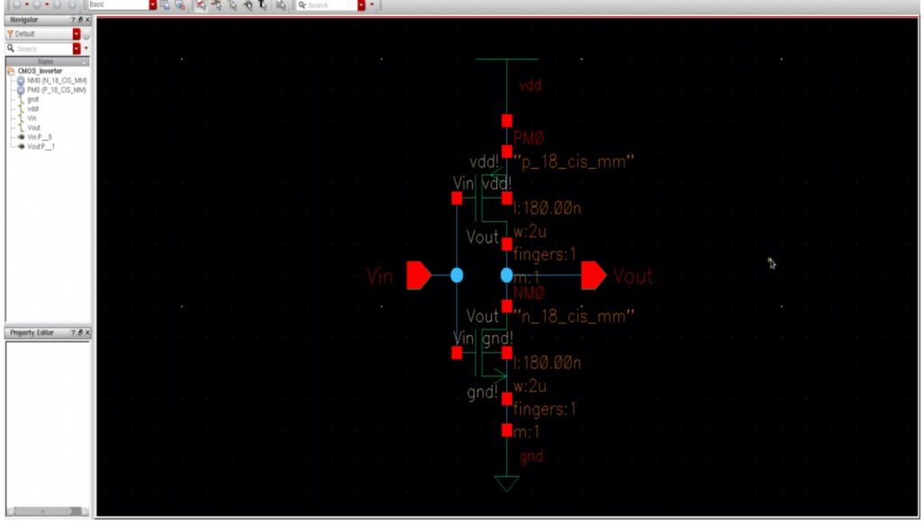
- You will create a new cell called “Inverter” with the schematic view and hence build the inverter schematic by instantiating various components. Once inverter schematic is done, a symbol for “Inverter” is generated. Now you will create a new cell view called “Inverter_Test”, where you will instantiate the “Inverter” symbol.
- This circuit is verified by doing various simulations using specter. In the process you will learn to use spectre, waveform window options, waveform calculator, etc…
- You will learn the Layout Editor basics by concentrating on designing an “Inverter” through automatic layout generation. Then you will go ahead with completing the other layouts.
- After that, you will run DRC, LVS checks on the layout, Extract parasitic and back-annotate them to the simulation environment.
LAB GETTING STARTED:
1. Log in to your workstation using the username and password. Ex: username: student Password: student 2. After login, create a folder in the desired location and name it as “myDesign”, Right Click on the folder “myDesign” and choose Open in Terminal Option. This will ensure that you are directed to the folder my design and the respective environment variables to invoke the tools will be set. 3. To verify that the path to the software is properly set in the cshrcfile, type the below command in the terminal window and enter: >which virtuoso It gives the complete path of the IC tool Installation. >which spectre It gives the complete path of MMSIM tool Installation >which assura It gives the complete path of Assura tool Installation. >which ncsim It gives the complete path of IUS tool Installation. |
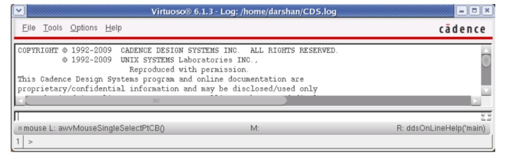
| Use the installed database to do your work and the steps are as follows: You will start the Cadence Design Framework II environment from the directory “saveetha” by entering the below commands in a terminal. > right-click on Desktop and open a Terminal >mkdirmyDesignLib >dmyDesignLib In the same terminal window, enter: > virtuoso& The virtuoso or Command Interpreter Window (CIW) appears at the bottom of the screen:- |
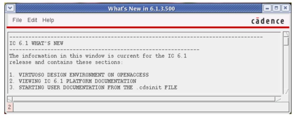
- If the “What‟s New …” window appears, close it with the
File— Close command.
Keep open the CIW window for the labs.
Lab 1: AN INVERTER:-
Related posts:
 Cadence Tutorial 2
 ELECTRONIC DESIGN AUTOMATION (EDA) USING CADENCE
 PCB Design internship, Qmax systems (ECE/EEE), Chennai, India
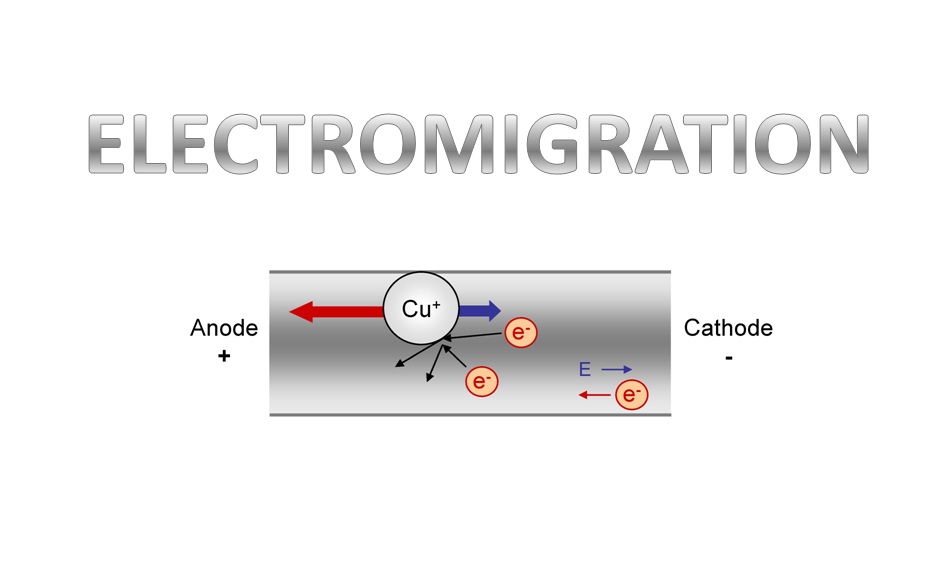 mechanisms in Integrated circuits
 Introduction to Boolean Algebra and Fundamentals of Logic Gates
 GATE-2021 Syllabus vs GATE -2020 Syllabus for EC (Electronics and Communication)
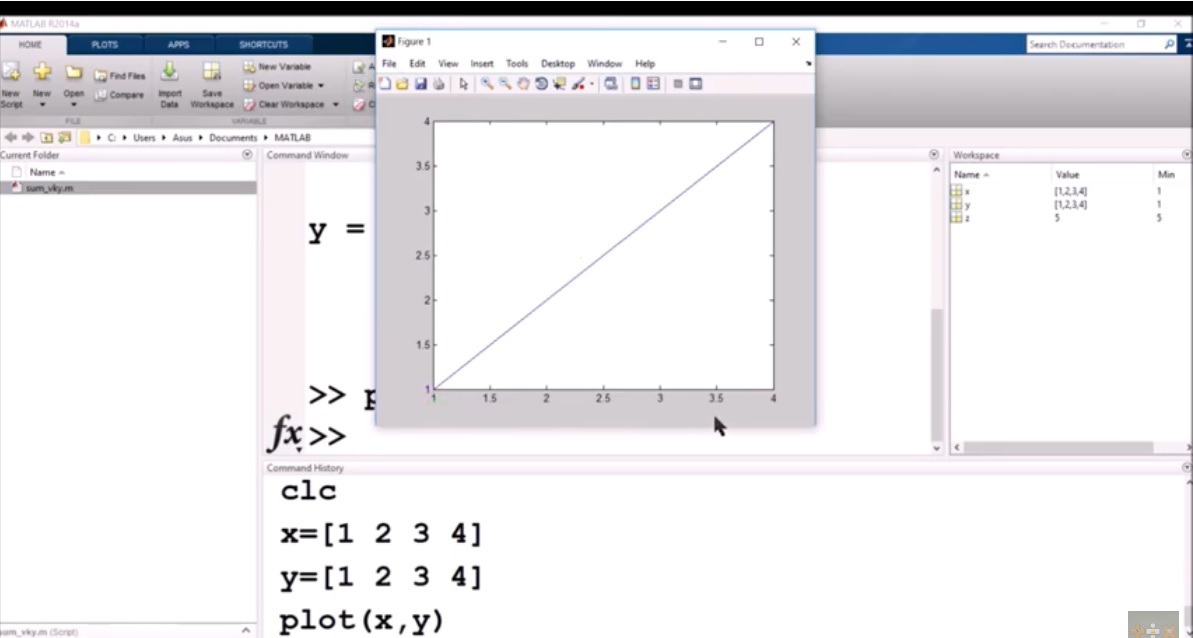 MATLAB A POWERFUL TOOL FOR THE ENGINEERS