

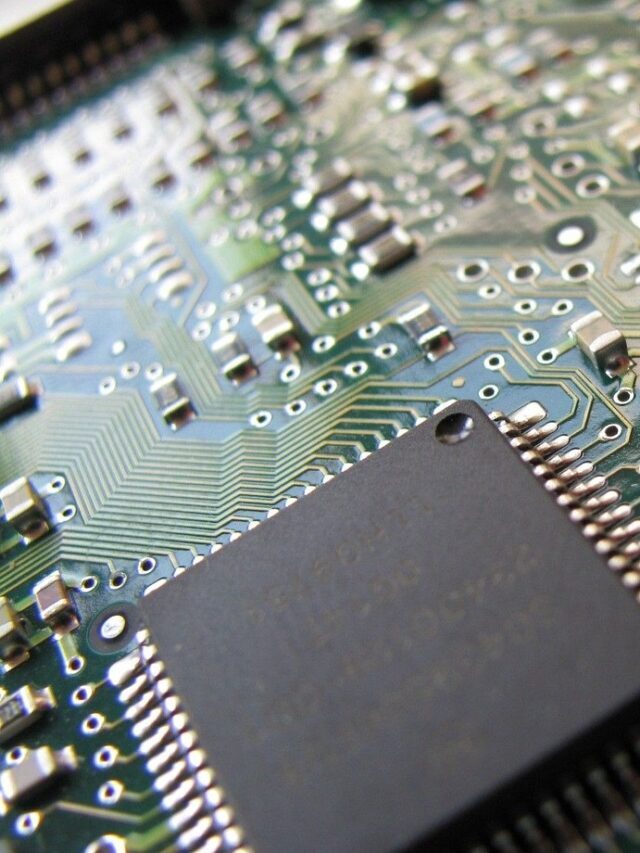

Testing a VLSI (Very Large Scale Integration) design block is a multistep process aimed at ensuring its functionality and performance.
The testing process involves the following key steps:
Pre-silicon Verification:
Before fabrication, the design undergoes extensive simulation using tools such as Verilog or VHDL simulators. This step helps identify and rectify design flaws and logic errors early in the development process. Click Here for Detailed article
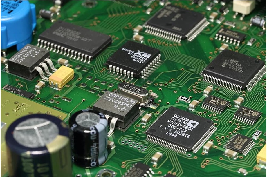
Post-silicon Validation:
After fabrication, the chip is tested using specialized equipment to verify its functionality under real-world conditions. Various test patterns and stimuli are applied to the chip to validate its functionality.
Scan Testing:
Scan chains are integrated into the design to enable the testing of internal logic paths. This allows for the application of test patterns and the observation of internal signals, aiding in fault detection.
Built-In Self-Test (BIST):
BIST circuits are integrated into the design to enable self-testing of the block. This can include memory BIST (mBIST) for testing embedded memory and logic BIST for testing logic circuits.
Fault Simulation:
Fault simulation is utilized to test the design’s resilience against faults such as stuck-at, bridging, and delay faults. This ensures that the design functions correctly in the presence of manufacturing defects.
Design for Testability (DFT):
DFT techniques are employed during the design phase to enhance the block’s testability. This may involve incorporating scan chains, BIST circuits, and other testability features.
Post-silicon Debugging:
In case faults are detected during testing, post-silicon debugging techniques are employed to locate and rectify the faults. This may involve using specialized equipment and techniques to analyze the chip’s behavior.
In conclusion, testing a VLSI design block is a complex process that necessitates meticulous planning and execution to ensure that the final product meets its specifications.
Related posts:
 SoC/IP Pre-silicon verification of VLSI Design
 Design Verification Interview Question with Answer-Part-1
 GATE-2021 Syllabus vs GATE -2020 Syllabus for EC (Electronics and Communication)
 Odisha Semiconductor Design Challenge (Last Date: 30-11-2023)
 What is System on Chip (SoC) ?
 What is PCB (Printed Circuit Board)?
 Introduction to Boolean Algebra and Fundamentals of Logic Gates
 Various Internship Opportunities @Intel, India for B.E./B.Tech./M.E./M.Tech/MS