


Argus Embedded System, Hyderabad, Telangana
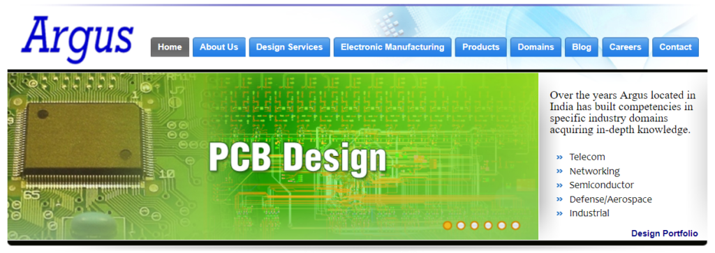
Over the years Argus located in India has built competencies in specific industry domains acquiring in-depth knowledge.
- Telecom
- Networking
- Semiconductor
- Defense/Aerospace
- Industrial
Sr. Hardware Design Engineer (Location: Hyderabad, India)
Job Responsibilities:
The job involves working on high-speed board designs for networking, broadband and communication products
You will be involved in all phases of the development including the specification, schematic capture, layout review, mechanical design review, and hands-on board debug and testing.
You will be interfacing with various functional groups including software designers, test engineers, and marketing. The scope includes Support for software integration testing and product support to customers.
Skills & Experience:
- Proficiency in High-speed multi-layer Board design with network processors, DSP or micro-controllers.
- Knowledge and experience of working on High-end processor-based architectures, FPGA’s and multi-board systems will be essential.
- It’s essential for the candidate to have strong application knowledge and board debugging skills.
- Must have a good working knowledge of schematic entry (Orcad/view logic) and PCB layout tools (PADS/allegro)
- You must be a self-starter requiring minimal supervision. You must also be a good team player with good communication skills, with a good track record of meeting tight schedule commitments.
Sr. FPGA Design Engineer (Location: Hyderabad)
Job Responsibilities:
- Must be a post-graduate/undergraduate in ECE/Electronics from a reputed engineering college/Institute.
- Must be very good in Verilog programming/Debugging/able to write synthesizable codes.
- A very good understanding and hands-on working level experience in basic digital building blocks/logic modules.
- Must have worked in top-level SoC integration of processor cores with standard Peripherals. Must have exposure to communication protocols Must have solid working level experience in ModelSim/VCS and other industry-standard simulator tools.
- Should be very good in the debugging the HDL codes and be able to make progress by identifying and fixing the issues/bugs in the design.
- Working-level experience in the standard FPGA architectures, FPGA based system design, IP development
- Need to take independent responsibilities/activities. Exposure on C/C++ based programming/ Perl scripts/basic c shell scripting languages are desirable.
Jr. FPGA Design/Verification Engineer (Location: Hyderabad)
Job Responsibilities:
- Should have at least 6 months to 1-year exp, in FPGA RTL (mostly Verilog) design, architect understanding debugging and synthesis exp
- Exp. In Xilinx/ISE latest version is a must.
- Should be a good team player, able to work smoothly with the other team member
- Should be prepared to work with h/w board-level design and board bring-up team (in case needed).
- Having some basic knowledge on h/w such as ADC, DAC, basic digital design ICs, micro-controller and USB/UART/SPI i/f and memory devices.
- Candidates should have ECE, Electronics or VLSI design in their curriculum & after their graduation/PG need to have undergone yr. course on FPGA/VLSI.
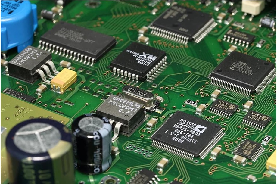
PCB Layout Engineer (Location: Hyderabad)
Job Responsibilities:
PCB Design Engineer with experience in one or more of the industry-standard PCB layout packages. Experience in schematic capture and Experience in circuit design fundamentals is added advantage
Skills & Experience:
- Responsible for PCB design layout for new FPGA and microprocessor-based multi-layer designs.
- Create components footprints based on datasheets
- Coordinate board planning, layout, post-processing
- Participate in hardware design meetings and provide inputs/feedback
- Required Experience, Skills and Qualifications
- Expertise in at least one PCB Cad Software
- Good understanding of Electronic Circuits & Electronic components
- Vision for Design for manufacturing methodology
- Ability to understand data sheets
- Ability to create component footprints
- Ability to evaluate and select optimal component packages
- Strong ability to anticipate possible problems and fix them before the design is rolled out for manufacturing
- Good knowledge in EMI EMC fundamentals
Company Address:
Hyderabad Plot No. 36, Phase-III, 1st Floor, Kamalapuri colony Hyderabad Telangana, Hyderabad, 500073
India: +91-7093535378
Website: http://www.sysargus.com/index.php
Career page: http://www.sysargus.com/careers.php
Related posts:
 What is PCB (Printed Circuit Board)?
 PCB Design Job @ Inch Group, Gurgaon (Haryana)
 SOC Verification Engineer (Power Management)
 PCB Design internship, Qmax systems (ECE/EEE), Chennai, India
 FPGA Software Validation Engineer – Intern@Intel
 Senior Android Developer@Asiczen Technologies, Bhubaneswar [Urgent Requirement]
 Xenius Job Opportunity
 EC/EI/CS/IT/(Embedded) Project Engineer (against Advertisement No. CDAC/Noida/03/August/2019 Noida Recruitment