

ELECTRICAL OVERSTRESS
- Electrical Overstress (EOS) is a term refers to failures caused by the application of excessive voltages or currents to a component.
- Electrical overstress is a phenomenon where electrical signals applied to a circuit or a device exceeds normal operating parameters.
- These excessive electrical signals are abnormal by definition and are not a part of the normal operation of the devices.
- It is a substantial threat to components in the production environment.
- According to Intel, EOS is the number one cause of damage to IC components.
- An EOS event can be a momentary event lasting only milliseconds or can last as long as the conditions persist. EOS can be the result of a single non-recurring event or the result of ongoing periodic or non-periodic events.
- In order to avoid EOS fails right from the beginning of the IC design process, a methodology is:
There are five common types of EOS failures:-
- Electromigration
- Antenna Effect
- Latch-up
- Matching
- Crosstalk.
Electromigration:
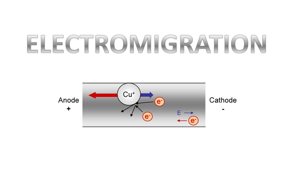
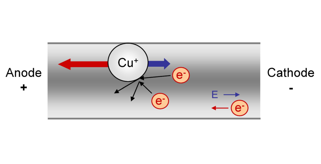
- Electromigration is the transport of material caused by the gradual movement of the ions in a conductor due to the momentum transfer between conducting electrons and diffusing metal atoms.
- It occurs when the current density is high enough to cause the drift of metal ions in the direction of the electron flow and is characterized by the ion flux density.
- This density depends on the magnitude of forces that tend to hold the ions in place.
- Electromigration is slow wear out phenomenon caused by extremely high current densities. In Aluminium, electromigration only becomes a concern when current densities approach 5×10^5 A/cm^2.
Cause of Electromigration:
- Electromigration was encountered in high-density digital logic.
- As the dimensions of the Integrated Circuits were progressively reduced, the current density flowing through the metallization increased.
- Some devices eventually exhibited open-circuit metallization failures after many thousands of hours of operation at elevated temperatures.
- Carriers flowing through the metal collide with the lattice atoms.
- At current densities in excess of several million amps per square centimeter, these impacts become so frequent that the metal atoms begin to move.
- The displacement of the atoms causes voids to form between individual grains of the polycrystalline metal aggregate. Eventually, these voids grow together to form a gap across the entire lead, causing an Open-Circuit failure.
- Electromigration causes metal atoms to gradually move away from the grain boundaries, forming voids between adjacent grains. This causes a decrease in the lead‟s effective cross-sectional area and raises the current density seen by the remainder of the lead. Additional voids form and gradually coalesce (to grow together) until they ultimately sever (to break off) the lead.
Related posts:
 What is PCB (Printed Circuit Board)?
 GATE-2021 Syllabus vs GATE -2020 Syllabus for EC (Electronics and Communication)
 Cadence Tutorial 2
 TCS CodeVita Season 9, 2020
 Xenius Job Opportunity
 PCB Design internship, Qmax systems (ECE/EEE), Chennai, India
 Software Engineering Intern @Microsoft(CSE/IT/ECE/EEE/E&I)