


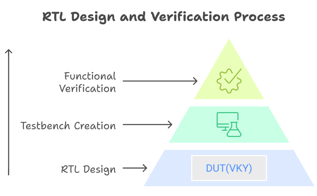
Step 1 : RTL Design (Verilog for 2-bit Adder)
RTL stands for Register Transfer Level. It’s a way of designing digital circuits — like processors, adders, or controllers — by describing how data moves between registers and what operations are performed on that data.
module adder_2bit (
    input  [1:0] a,
    input  [1:0] b,
    output [2:0] sum
);
    assign sum = a + b;
endmodule
Explanation :
This RTL code describes a simple 2-bit binary adder in Verilog. It defines a module named adder_2bit that takes two 2-bit input values, a and b, and produces a 3-bit output called sum. The assign statement performs the addition operation a + b, and stores the result in sum. The output is 3 bits wide to account for any carry that might occur when the two 2-bit numbers are added, ensuring no data is lost. This module represents a basic example of how arithmetic operations can be expressed at the Register Transfer Level, describing the behavior of a digital circuit.
Step 2 : Testbench for Functional Verification
A testbench for functional verification is a piece of code written to simulate and test an RTL design, ensuring that the circuit behaves correctly under different input conditions. It acts like a virtual lab setup where the RTL module is connected, given various input combinations, and its outputs are checked. The testbench does not become part of the final hardware; instead, it is used during simulation to verify the functionality of the design before it’s synthesized or manufactured. Without a testbench, there’s no reliable way to confirm whether the RTL code performs as intended, which makes it a crucial step in the digital design verification process.
module tb_adder_2bit;
    reg  [1:0] a, b;
    wire [2:0] sum;

    adder_2bit uut (.a(a), .b(b), .sum(sum));

    initial begin
        $display("a b | sum");
        for (int i = 0; i < 4; i++) begin
            for (int j = 0; j < 4; j++) begin
                a = i; b = j;
                #1;
                $display("%0d %0d | %0d", a, b, sum);
            end
        end
        $finish;
    end
endmodule
Explanation :
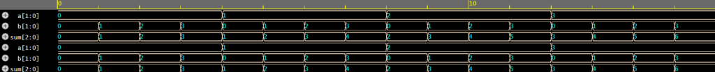
This SystemVerilog testbench module, tb_adder_2bit, is designed to verify the functionality of a 2-bit adder named adder_2bit. It declares two 2-bit input registers a and b, and a 3-bit wire sum to hold the addition output. The adder module is instantiated using uut (unit under test), connecting its ports to the testbench signals. Inside the initial block, a nested loop iterates through all possible combinations of 2-bit values for a and b (from 0 to 3), assigns them, waits for a simulation time unit, and prints the input and resulting sum. This helps verify that the adder correctly computes the sum for every input combination.
=================
Output:
=================
a b | sum
0 0 | 0
0 1 | 1
0 2 | 2
0 3 | 3
1 0 | 1
1 1 | 2
1 2 | 3
1 3 | 4
2 0 | 2
2 1 | 3
2 2 | 4
2 3 | 5
3 0 | 3
3 1 | 4
3 2 | 5
3 3 | 6
============
Wave:
Step 3: Synthesis
Synthesis is a crucial step in digital design where the RTL (Register Transfer Level) code written in hardware description languages like Verilog or VHDL is converted into a gate-level netlist. This netlist is a representation of the circuit using logic gates and flip-flops that a physical device like an FPGA or ASIC can understand. During synthesis, the design is optimized for speed, area, and power by mapping the code onto technology-specific components (like lookup tables in FPGAs or standard cells in ASICs).
Why is it required?
RTL code is abstract and not directly implementable in hardware. Synthesis bridges the gap between your high-level code and the physical hardware by translating your behavioral design into actual logic circuits that follow the target technology constraints.
Necessity of Synthesis
Without synthesis, the design remains just a simulation model. It cannot be fabricated or deployed on real hardware. Synthesis ensures that the design is logically correct, meets performance goals, and adheres to physical limitations of the chip or FPGA.
What if you skip synthesis?
Skipping synthesis means the design can never be implemented on a chip or tested in a real environment. You could simulate and verify the logic behaviorally, but you wouldn't know if it works within actual hardware constraints or how it performs in real-time. This makes the design practically unusable for deployment.
In summary, synthesis is essential to transform a high-level design into a form that can be physically realized, optimized, and eventually manufactured or programmed onto a device.
- Use Synopsys Design Compiler or Yosys to synthesize the design.
- Constraints (SDC) will define clock and timing requirements.
- Output will be a gate-level netlist.
Using Yosys (Open-Source Flow)
🔹 Step 3.1: Install Yosys
If not installed:
bash
CopyEditsudo apt install yosys   # On Ubuntu
🔹 Step 3.2: Create a Yosys Script (synth.ys)
tcl code:
===================================
CopyEdit# synth.ys - Yosys Synthesis Script
read_verilog adder_2bit.v
synth -top adder_2bit
write_verilog -noattr adder_2bit_synth.v
==================================
🔹 Step 3.3: Run the Script
bash
CopyEdityosys synth.ys
Gate-Level Netlist Version (Simplified, No Real Library Cells):
This is after synthesis — showing basic logic only:
Output:
You’ll get a synthesized gate-level netlist called adder_2bit_synth.v as shown below.
module adder_2bit (a, b, sum);
  input [1:0] a;
  input [1:0] b;
  output [2:0] sum;

  wire c0, c1;

  xor (sum[0], a[0], b[0]);                // sum[0] = a0 XOR b0
  and (c0, a[0], b[0]);                    // carry0 = a0 AND b0

  xor (sum[1], a[1], b[1], c0);            // sum[1] = a1 XOR b1 XOR carry0
  wire t1, t2, t3;
  and (t1, a[1], b[1]);                    // temp carry terms
  and (t2, a[1], c0);
  and (t3, b[1], c0);
  or  (c1, t1, t2, t3);                    // carry1 = majority vote
  assign sum[2] = c1;                      // sum[2] = carry out

endmodule
Simulation with Synthesized Netlist
Once the RTL code has been synthesized into a gate-level netlist (often in the form of a .v or .edf file), it represents the design as a network of logic gates, flip-flops, and other low-level components. This netlist can be simulated, but the simulation at this level is generally more focused on the post-synthesis behavior, which reflects how the design will perform after it has been mapped onto actual hardware, as opposed to simulating the original high-level RTL code.
Types of Simulations with Synthesized Netlist
- Post-Synthesis Simulation:
- Purpose: This simulation is used to verify that the synthesized design behaves as expected after the synthesis process. It ensures that no errors were introduced during synthesis (e.g., logic optimizations or technology-specific changes).
- Tool: Typically, you would use simulation tools like ModelSim, QuestaSim, or VCS to run post-synthesis simulations with the netlist. These tools allow you to simulate gate-level behavior, including delays and timing characteristics.
- Behavioral Simulation:
- Purpose: Before synthesis, you typically simulate the RTL code (behavioral level) to check its logical correctness. This step can catch most design errors early on, but post-synthesis simulation is necessary for confirming that the logic works as intended at the hardware level.
- Tool: For behavioral simulation, you use the same tools (ModelSim, QuestaSim, etc.), but you work with the original RTL code.
Necessity of Post-Synthesis Simulation
- Timing and Gate-Level Analysis: The synthesized netlist incorporates all timing, area, and power constraints. By running a simulation on the netlist, you get a more accurate picture of how the design will behave on real hardware, considering delays and propagation times that don’t exist in RTL simulation.
- Verification Against Constraints: Post-synthesis simulation helps in verifying that the design meets the required timing constraints (like setup/hold times) and that no timing violations or issues have been introduced during synthesis.
What Happens if You Skip Post-Synthesis Simulation?
Skipping this simulation step means you won't know if your design functions as intended when mapped onto actual hardware. Even if your RTL code passes simulation successfully, the synthesized netlist might have issues like timing violations, which can only be detected after synthesis. Therefore, skipping this step can lead to bugs and functional problems in the hardware that might not appear in RTL simulations.
Technology-Mapped Netlist (Real Cell Example)
After synthesis with a real cell library like SAED90nm, your
A Technology-Mapped Netlist refers to the netlist where the logic gates have been mapped to specific standard cells of a given technology. These standard cells are pre-designed, optimized cells provided by the semiconductor manufacturer or design library for a specific process node (e.g., 28nm, 7nm). These cells are the building blocks used to implement the design on a physical chip.
To generate a Technology-Mapped Netlist, the following steps are typically followed:
- Choose the Target Technology:
Select the appropriate technology library that corresponds to the process node you’re targeting (e.g., 28nm, 7nm). These libraries contain predefined standard cells, such as logic gates (AND, OR, XOR, etc.), flip-flops, multiplexers, and other essential components. - Synthesis with Technology Library:
- After writing the RTL code (in Verilog/VHDL), the next step is synthesis. During synthesis, the tool maps the abstract RTL design to actual cells in the chosen technology library. This step involves converting the high-level logic into a netlist of standard cells.
- Tools like Synopsys Design Compiler, Cadence Genus, or Xilinx Vivado can perform this mapping. These tools take the RTL code and the technology library as inputs, optimizing the design for area, speed, and power.
- Post-Synthesis Optimization:
Once the initial netlist is generated, various optimizations are performed. These optimizations aim to minimize the area, reduce power consumption, and meet the performance goals for the design. These optimizations are performed at the gate level, but the gates used are real physical cells (from the standard cell library). - Output Technology-Mapped Netlist:
The result of the synthesis process is a technology-mapped netlist, which consists of real cells from the library, connected together to implement the logic described by the RTL code. The technology-mapped netlist includes detailed information on the specific type of cell (e.g., a 2-input AND gate, flip-flops, buffers) used to realize the design.
The netlist will look like:
module adder_2bit (a, b, sum);
  input [1:0] a;
  input [1:0] b;
  output [2:0] sum;

  wire n1, n2, n3, n4;

  XOR2X1 U1 (.A(a[0]), .B(b[0]), .Y(sum[0]));
  AND2X1 U2 (.A(a[0]), .B(b[0]), .Y(n1));

  XOR3X1 U3 (.A(a[1]), .B(b[1]), .C(n1), .Y(sum[1]));

  AND2X1 U4 (.A(a[1]), .B(b[1]), .Y(n2));
  AND2X1 U5 (.A(a[1]), .B(n1), .Y(n3));
  AND2X1 U6 (.A(b[1]), .B(n1), .Y(n4));
  OR3X1  U7 (.A(n2), .B(n3), .C(n4), .Y(sum[2]));

endmodule
If you want timing analysis, you’ll also need to write an SDC file:
tcl
==============================
create_clock -period 10 [get_ports clk]
set_input_delay 2 [all_inputs]
set_output_delay 2 [all_outputs]
==============================
Step 4: DFT Insertion
DFT stands for Design for Testability. It’s a technique used in digital design to make it easier to test a chip once it's been fabricated. After synthesis (where the RTL code is converted into a technology-mapped netlist), DFT insertion is performed to add extra circuitry that helps test the chip more effectively during manufacturing.
Why is DFT Insertion Required?
After synthesis, the design is mapped onto real cells, and at this stage, it's important to ensure that the chip can be tested once it's physically made. Testing is crucial to catch defects or errors in the manufacturing process. Without DFT, testing the individual parts of the chip, like logic gates and flip-flops, could be very difficult and time-consuming.
Key reasons why DFT is required:
- Ensure Manufacturing Quality: Detect faults or manufacturing defects, like stuck-at faults or open circuits, that may occur when producing the chip.
- Test Coverage: Help cover all the parts of the chip (even those not directly accessible) to ensure the design functions as intended.
- Minimize Cost: With proper DFT insertion, the chip can be tested using automated tools, reducing manual testing effort and speeding up the process.
- Improve Debugging: If a design fails in the real world, DFT provides helpful information to pinpoint where the issue is within the chip.
How is DFT Insertion Done?
- Scan Chain Insertion:
- The most common DFT technique is scan insertion. Here, scan chains are added to the design, which are sequences of flip-flops connected in a way that allows them to be accessed and controlled from outside the chip.
- This allows testers to shift data into the flip-flops, control the chip’s state, and check the outputs, making it easier to find faults. This is done by inserting scan cells (specialized flip-flops with test ports) into the design.
- Insert Built-In Self-Test (BIST):
- Sometimes, a design might include a BIST (Built-In Self-Test) feature, where the chip can run a self-test to check for faults. This is especially useful for complex chips where external test equipment may not be practical.
- Boundary Scan:
- Boundary scan (often used in combination with scan chains) allows testing of the chip's pins (input/output pads) and the connections between them. This is like running a test on the "boundary" of the chip to check if the inputs and outputs work correctly.
- Test Coverage and Control Logic:
- After scan chains or other test circuits are inserted, you can control which parts of the design are being tested at any given moment. Tools like Synopsys DFT Compiler or Cadence Modus help automate this process by adding the necessary test circuitry.
- The test logic might include MUXes (multiplexers) that allow test signals to be injected into the design and observation points to monitor the results.
- Inserting the DFT Logic:
- DFT insertion is typically done by EDA (Electronic Design Automation) tools. These tools take the synthesized netlist and automatically add the required scan chains, control logic, and observation points.
- After insertion, the design is still logically the same, but now it has additional test features built into it for easier verification.
Summary of the Process:
- Before DFT: You have a synthesized netlist, which is just the design mapped to standard cells without testability features.
- During DFT Insertion: You add test structures like scan chains, BIST logic, and boundary scan to ensure that the chip can be tested automatically once it’s manufactured.
- After DFT: The design has testability features that allow it to be verified for faults and defects, making the chip easier to debug and verify in real-world conditions.
Why is DFT Important?
Without DFT, testing the chip would require complex manual inspection and testing of every part of the chip, which is costly, time-consuming, and error-prone. DFT makes the process of testing automated and efficient, which is critical when chips have millions or even billions of components.
Use DFT tools like Synopsys DFT Compiler or Mentor Tessent:
- Insert scan chains by converting flip-flops to scan DFFs.
- Create scan-in and scan-out ports.
- Generate a DFT netlist.
Insert Scan Chains by Converting Flip-Flops to Scan DFFs:
This involves replacing regular flip-flops (DFFs) in the design with scan flip-flops (Scan DFFs) that allow easy access to their internal states during testing. These scan DFFs are connected to form a scan chain for testing purposes.
Create Scan-In and Scan-Out Ports:
Scan-in and scan-out ports are added to the scan chain to provide external access for injecting test data into the scan chain and observing the outputs, facilitating easier testing.
Generate a DFT Netlist:
After inserting the scan chains and test structures, a DFT (Design for Testability) netlist is generated. This netlist includes the necessary test circuitry (scan chains, scan-in/out ports, etc.) to ensure the design can be effectively tested post-silicon.
This step adds:
- Scan-enable (
scan_en) - Scan-in (
scan_in) - Scan-out (
scan_out)
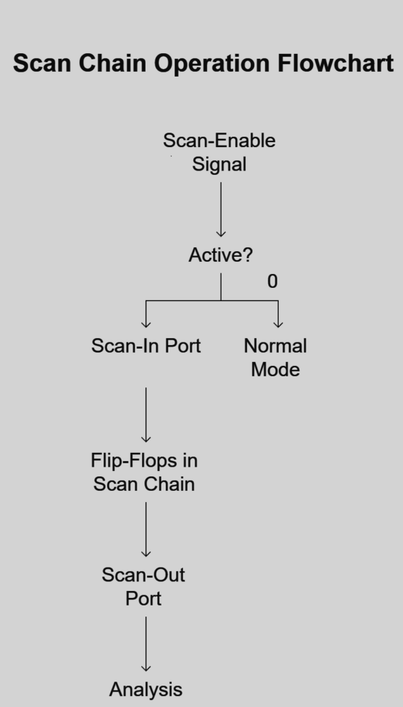
Scan-Enable (scan_en):
This signal controls whether the circuit operates in normal mode (functional mode) or scan mode (test mode). When scan_en is active (usually 1), the flip-flops in the scan chain are connected to the scan inputs and outputs for testing. When inactive (0), the flip-flops behave normally and store data as per the design's logic.
Scan-In (scan_in):
The scan-in port is the entry point for test data into the scan chain. It allows the external tester to inject data into the first flip-flop of the scan chain, which then shifts through the rest of the flip-flops for testing.
Scan-Out (scan_out):
The scan-out port is the exit point where the results of the scan chain are observed. After the scan-in data has propagated through the chain and the design is tested, the results can be read out via the scan-out port for analysis.
Step 5: DFT Verification
DFT Verification is a critical step that ensures the Design for Testability (DFT) structures and logic inserted into the design function correctly. After DFT is inserted into the design, it’s crucial to verify that these test structures are working as expected and do not interfere with the normal operation of the chip. This step is usually done before the design proceeds to physical implementation (place-and-route) and fabrication.
Steps to verify:
- Write testbenches to apply scan vectors:
- Create simulation code to load test patterns into the scan chain and observe outputs.
- Verify stuck-at fault models:
- Ensure the design can detect faults where signals are stuck at logic '0' or '1'.
- Check if scan chains are shifting correctly:
- Confirm that data moves properly through the scan flip-flops during shift operations.
- *Simulate using .vec or ATPG patterns:
- Use test pattern files generated by ATPG tools to simulate and validate scan functionality.
You’ll be verifying:
- Controllability (can you toggle the flip-flops through scan?)
- Observability (can you observe internal faults on scan_out?)
- Pattern correctness (pass/fail logic)
Controllability:
This checks if you can set or toggle the flip-flops using scan-in data, ensuring that all flip-flops in the scan chain are reachable for testing.
Observability:
This ensures that any internal fault (like stuck-at faults) can be seen at the scan-out pin, making internal logic errors detectable during testing.
Pattern Correctness:
This verifies whether the applied scan test patterns produce expected outputs. A mismatch indicates a fault (fail), while correct output means the test passed.
Step 6: ATPG (Automatic Test Pattern Generation)
ATPG stands for Automatic Test Pattern Generation. Think of it like a smart tool that creates special input patterns to check whether a chip has any manufacturing defects.
After inserting scan chains into your design, ATPG software is used to automatically generate test vectors—these are sequences of 1s and 0s sent into the chip to test different parts of it. The goal is to find faults like wires stuck at 0 or 1, which can happen during chip fabrication.
Instead of manually figuring out what inputs to use for testing, ATPG does this work for you. It ensures that every gate and connection inside the chip is tested properly. It also checks whether faults can be controlled (input values can reach them) and observed (the result can be seen at the output).
In short, ATPG helps verify the health of your chip before it reaches the market, making sure that all testable faults are covered efficiently.
- Use tools like TetraMAX or FastScan to generate test patterns
- Patterns detect stuck-at, transition, and path delay faults
- These are later simulated for fault coverage reporting
To begin, I would use DFT tools like TetraMAX or FastScan to generate test patterns for the RTL or synthesized netlist. These patterns are automatically created by the tool to target various fault models — most commonly stuck-at faults, transition faults, and path delay faults. Each fault type helps in detecting specific manufacturing or timing issues in the chip. Once the patterns are generated, they are simulated using the same tool or a supported simulator to evaluate how effectively the test vectors can detect faults. This is known as fault simulation, and it produces a fault coverage report, showing the percentage of possible faults that can be detected. Based on this report, we can refine the design or improve scan insertion to reach higher fault coverage, ensuring a more reliable and testable chip design.
Step 7: Post-DFT Simulation & Coverage
- Run patterns on the gate-level netlist
- Measure fault coverage
- Report any redundant or undetected faults
In this step, the generated DFT test patterns are applied to the gate-level netlist of the design (i.e., the netlist after scan insertion and synthesis). This process is known as post-DFT simulation, where the actual fault models (like stuck-at or transition faults) are simulated using the inserted scan logic. The goal is to measure fault coverage, which represents the percentage of targeted faults that are detected by the patterns. The tool then generates a coverage report, which highlights how effective the patterns are. It also identifies any redundant faults (which are impossible to detect due to the design's structure) and undetected faults (which may require better pattern generation or design changes). This step is crucial for ensuring that the chip can be reliably tested during manufacturing.
Step 8: Optional: Physical Design + Signoff
After successful RTL design, synthesis, and DFT insertion, the next phase in the full chip flow is often Physical Design — the process of translating the logical design into a physical layout that can be fabricated on silicon. This includes steps like floorplanning, placement, clock tree synthesis (CTS), routing, and finally signoff checks such as timing analysis, power analysis, and design rule checking (DRC). Signoff ensures that the final layout meets all physical, electrical, and performance constraints set by the foundry.
Physical Design is labeled optional here because your project (a 2-bit adder with DFT) is likely being done for academic, learning, or prototyping purposes — where functional verification, synthesis, and DFT flow are the main focus. Full physical implementation and signoff require additional tools, foundry files, and extensive effort, which may not be necessary for small-scale or educational projects. However, in real chip development, this step is mandatory before tape-out.
If you want to go beyond:
- Place & route using Cadence Innovus or OpenROAD
- Run STA to check setup/hold violations
- Generate GDSII for tape-out
To take your design all the way to fabrication, you can proceed with Place & Route using industry tools like Cadence Innovus or open-source alternatives such as OpenROAD. In this step, your synthesized netlist is physically implemented by placing standard cells on a chip layout and routing wires to connect them. After placement and routing, the design must be validated through Static Timing Analysis (STA) — a process that checks whether the design meets all setup and hold time constraints at all paths and corners. Violations here can cause timing failures, so they must be fixed before proceeding.
Once STA passes, the final step is to generate a GDSII file — the standard format used to describe the physical layout of the chip. This GDSII file is what is sent to the foundry for tape-out, which means the chip is ready to be manufactured.
Related posts:
 DFT Verification Interview Questions with answers Part-1
 Design Verification Interview Question with Answer-Part-1
Mailbox in System Verilog
Solutions of FPGA Design Engineer Interview Question Part-1
Semaphore in System Verilog
Design Verification Interview Question with Answer-Part-1
Mailbox in System Verilog
Solutions of FPGA Design Engineer Interview Question Part-1
Semaphore in System Verilog
 SoC/IP Pre-silicon verification of VLSI Design
 How to Test a VLSI Design Block?
 Introduction to System Verilog