


Registration Start Date 02-11-2023
Registration End Date 30-11-2023
Type – Open Challenge
Display – Flagship Events
Venue – Online Event
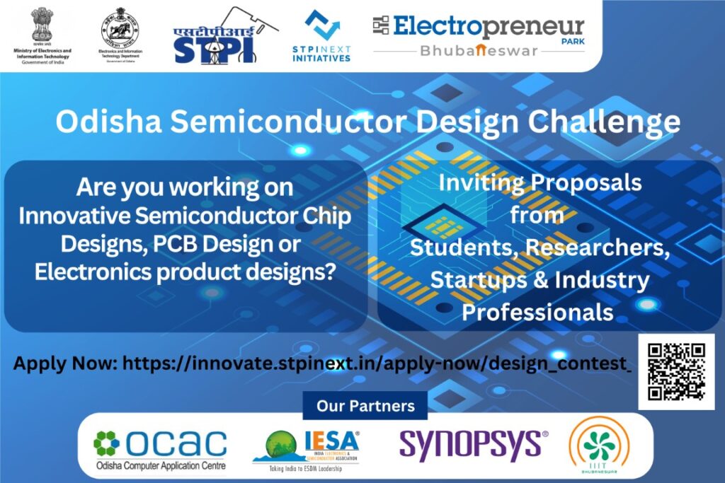
Electropreneur Park-Bhubaneswar, an ESDM CoE of Software Technolgy Parks of India with support from the Electronics & IT Department, Govt. of Odisha, Odisha Computer Application Centre (OCAC), IESA, Synopsis, and Industry Partners, is organising the contest “Odisha Semiconductor Design Challenge”.
This contest aims to give Students, Researchers, and Startups an avenue to showcase their abilities in developing innovative electronic products, Circuits, and Chip designs.
The participants will have the opportunity to demonstrate their skills in designing electronic products, Semiconductor Chips, etc. with the mentoring support from the stakeholders.
WHO CAN APPLY
- Students working on innovative electronic designs and Solutions
- Registered Start-ups
- Individual Academicians, Researchers, Educators, Entrepreneurs, Partnership firms, LLPs
FOCUS AREAS
- Agricultural Technologies
- EduTech
- Healthcare
- Energy/Power
- Communication
- Robotics
- Process Automation
- Any other Innovative sectors solving a critical problem statement
KEY TAKEAWAYS
- Cash Prize to the selected winners
- Opportunity for joint R&D with corporate houses, industry & academia
- Preferential access to State-of-the-art ESDM Lab and EDA Tools
- Strategic Guidance & Mentoring by Industry experts
- Rapid prototyping support
- Access to Fab Lab
- Pre-Incubation/Incubation opportunities
- Offer for Internship for School/College Students
PROBLEM STATEMENT
- Analog design
- Design of an On-Board Electric Vehicle charger for 2 wheelers
- Design of an autosar requirements-compliant RISC V processor design with integrated CAN bus.
- Design of an AI-based system for predicting crop tiled in all three seasons of harvesting in Odisha
- Any other innovative proposals in the field of System Design/Chip design
How to Apply : Click the button below to Apply online
Official Website : https://innovate.stpinext.in/
Importance of Semiconductor Design Challenge
- Introduction to Semiconductor Design Challenge
Semiconductor design challenges play a crucial role in driving innovation and pushing the boundaries of technological advancements. As the semiconductor industry continues to evolve and strive for greater efficiency, performance, and functionality, design challenges have become instrumental in harnessing the collective creativity and problem-solving skills of engineers and designers. These challenges not only foster a culture of innovation and collaboration but also bridge the gap between academia and industry. This article explores the importance of semiconductor design challenges, their impact on product development, and the trends shaping the future of this dynamic field.
- Introduction to Semiconductor Design Challenge
1.1 Understanding Semiconductor Design
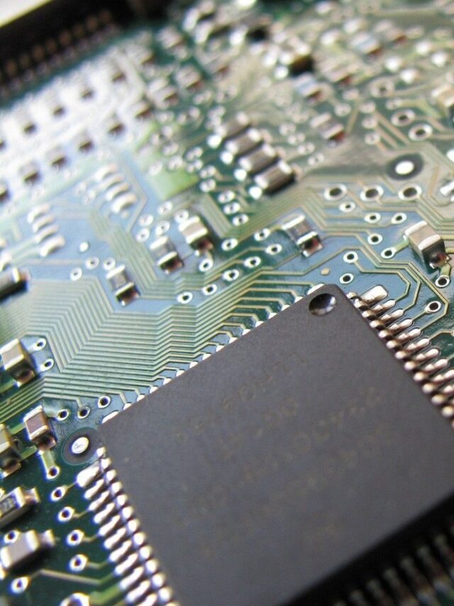
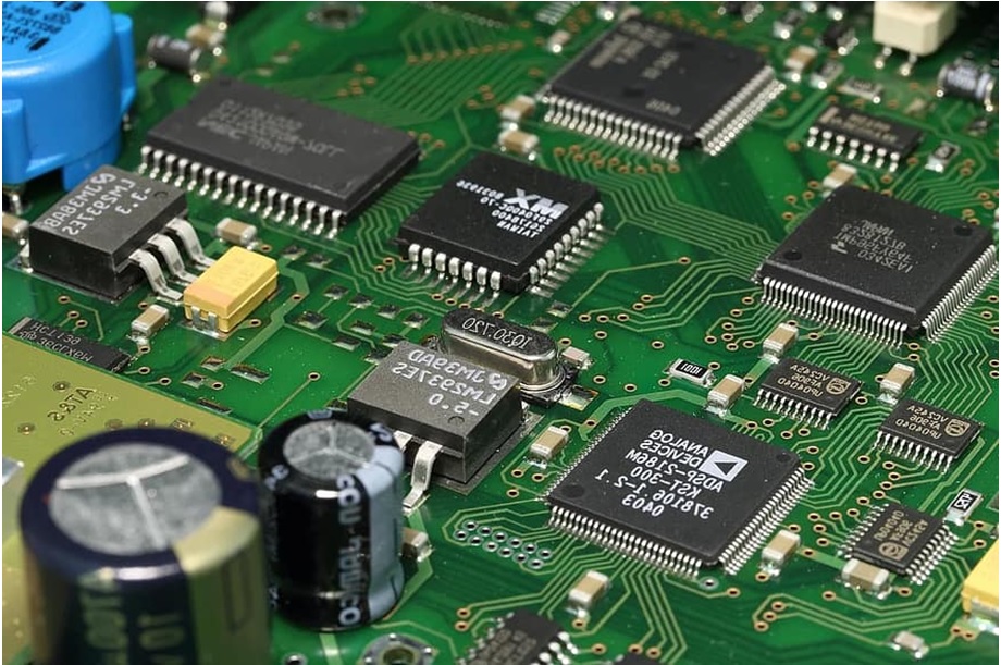
Semiconductor design is the process of creating integrated circuits that are the building blocks of modern electronics. It involves designing the layout, architecture, and functionality of these chips to ensure optimal performance and efficiency.
1.2 What is a Design Challenge?
A design challenge is a competition or project that challenges engineers and designers to solve a specific problem or create innovative solutions within a given timeframe. In the context of semiconductor design, it involves tackling complex problems related to circuitry, performance optimization, power management, and more.
- Advancements in Semiconductor Technology
2.1 Evolution of Semiconductor Technology
Semiconductor technology has come a long way over the years, revolutionizing the electronics industry. From early vacuum tubes to transistors and integrated circuits, advancements have led to smaller, faster, and more efficient devices.
2.2 Key Innovations in Semiconductor Design
Innovations in semiconductor design have been instrumental in driving technological progress. From the introduction of complementary metal-oxide-semiconductor (CMOS) technology to the development of FinFET and nanoscale transistors, these breakthroughs have paved the way for greater computing power and energy efficiency.
- The Role of Design Challenges in Semiconductor Industry
3.1 Importance of Design Challenges for Semiconductor Companies
Design challenges play a crucial role in the semiconductor industry as they encourage companies to push the boundaries of innovation. By participating in these challenges, companies can showcase their talent, gain recognition, and attract potential customers and investors.
3.2 Encouraging Collaboration and Creativity
Design challenges foster collaboration among engineers, designers, and students, creating a vibrant ecosystem for brainstorming and idea sharing. They provide a platform to explore unconventional approaches, leading to breakthroughs that may not have been possible through traditional design processes.
- Enhancing Innovation and Problem-Solving Skills through Challenges
4.1 Fostering a Culture of Innovation
Design challenges cultivate a culture of innovation within the semiconductor industry. They encourage participants to think outside the box, take risks, and explore new possibilities. This mindset fuels progress and drives the industry forward.
4.2 Developing Critical Problem-Solving Skills
Design challenges sharpen problem-solving skills by presenting participants with real-world engineering problems. Through these challenges, engineers learn how to analyze complex scenarios, consider trade-offs, and develop efficient and creative solutions. These problem-solving skills translate into enhanced professional growth and better-equipped engineers in the industry.
Odisha semiconductor design challenge has provided the problem statement in the following domain.
- Analog design
- Design of an On-Board Electric Vehicle charger for 2 wheelers
- Design of an autosar requirements-compliant RISC V processor design with integrated CAN bus.
- Design of an AI-based system for predicting crop tiled in all three seasons of harvesting in Odisha
- Any other innovative proposals in the field of System Design/Chip design
- Bridging the Gap between Academia and Industry
5.1 Integrating Design Challenges in University Curricula
When it comes to preparing students for the real world, textbooks can only take them so far. That’s where design challenges come in. By incorporating these challenges into university curricula, students get a taste of what it’s like to work in the semiconductor industry. It’s like taking ‘theory versus practice’ and turning it into a hands-on experience. Not only does this bridge the gap between academia and industry, but it also equips students with the practical skills and problem-solving mindset required in their future careers.
5.2 Benefits of Industry-Academia Collaboration
The beauty of design challenges is that they encourage collaboration between universities and industry professionals. This collaboration brings together the best of both worlds: the innovative and fresh perspectives of students, and the deep industry knowledge and experience of professionals. By working together, academia and industry can create design challenges that are relevant, cutting-edge, and reflective of the real-world challenges faced by semiconductor designers. This symbiotic relationship benefits students, industry professionals, and the semiconductor industry as a whole.
- Collaborative Learning and Networking Opportunities
6.1 Building Connections within the Semiconductor Community
Design challenges provide an excellent platform for students and professionals to network and build connections within the semiconductor community. In these challenges, individuals from different backgrounds and expertise come together, forming a diverse and collaborative environment. This not only fosters teamwork but also opens doors for future collaborations, mentorship opportunities, and even job prospects. So, not only are design challenges a chance to learn and grow, but they could also be the stepping stones to a bright future in the industry.
6.2 Sharing Knowledge and Best Practices
In the fast-paced world of semiconductor design, staying up-to-date with the latest trends and best practices is crucial. Design challenges provide a unique opportunity for participants to learn from each other and share their knowledge and experiences. Whether it’s discussing new design techniques, sharing tips for overcoming common obstacles, or showcasing innovative approaches, design challenges become a melting pot of ideas and insights. This collaborative learning environment benefits both students and professionals, and contributes to the overall advancement of semiconductor design.
- Impact of Semiconductor Design Challenges on Product Development
7.1 Accelerating Product Development and Time-to-Market
Time is money in the semiconductor industry, and design challenges can help speed up the product development process. The intense and time-constrained nature of these challenges pushes participants to think creatively and efficiently. As a result, they learn to streamline their design workflows, optimize performance, and effectively manage resources. By mastering these skills through design challenges, teams can bring their products to market faster, gaining a competitive edge in the industry.
7.2 Improving Product Performance and Efficiency
Design challenges are like laboratories for innovation. By pushing the boundaries of what’s possible, participants are encouraged to think outside the box and come up with novel solutions. Through these challenges, teams can discover new ways to improve product performance and efficiency. The practical experience gained from addressing real-world design problems fosters a mindset of continuous improvement, ultimately leading to better semiconductor products that meet the evolving needs of the market.
- Future Implications and Trends in Semiconductor Design Challenges
8.1 Emerging Technologies Shaping Design Challenges
As technology continues to advance, so do the challenges faced by semiconductor designers. Emerging technologies like artificial intelligence, Internet of Things, and quantum computing are reshaping the landscape of semiconductor design. Design challenges play a crucial role in preparing students and professionals to tackle these future challenges head-on. By incorporating these emerging technologies into design challenges, participants can gain valuable experience and stay ahead of the curve.
8.2 Predicting Future Challenges and Opportunities
The semiconductor industry is constantly evolving, and design challenges act as a barometer for what lies ahead. By analyzing the trends, patterns, and solutions that emerge from these challenges, industry professionals can gain insights into the future of semiconductor design. This knowledge helps companies identify potential challenges and opportunities, allowing them to adapt and innovate to stay competitive in the market. Design challenges serve as a crystal ball, providing a glimpse into the exciting possibilities that await in the world of semiconductor design. In conclusion, semiconductor design challenges have emerged as a vital catalyst for progress in the industry. By encouraging innovation, enhancing problem-solving skills, and fostering collaboration, these challenges have become instrumental in shaping the future of semiconductor technology. As we look ahead, it is clear that the impact of design challenges will continue to drive advancements, fuel product development, and pave the way for new technologies. Embracing these challenges and staying abreast of emerging trends will be key to staying at the forefront of the ever-evolving semiconductor landscape.
Related posts:
 IoT and Analysis with AWS and Azure Platforms (Short Term Training Program)
 AICTE SPONSORED ONE-WEEK ONLINE SHORTTERM TRAINING PROGRAMME(STTP) ON “Electronics Equipment Integration, Prototype Building and PCB Design”
 What is System on Chip (SoC) ?
 What is PCB (Printed Circuit Board)?
 SOC Verification Engineer (Power Management)
 Various Internship Opportunities @Intel, India for B.E./B.Tech./M.E./M.Tech/MS
 Trithon-2023 by Trident Group of Institutions ,Bhubaneswar
 Electronics Engineering Huge Opportunities Ahead in the Field of VLSI and Chip Design