electronics and telecommunication

How to Test a VLSI Design Block?

Post Views: 26 Testing a VLSI (Very Large Scale Integration) design block is a multistep process aimed at ensuring its functionality and performance. The testing process involves the following key steps: Pre-silicon Verification: Before fabrication, the design undergoes extensive simulation using tools such as Verilog or VHDL simulators. This step helps identify and rectify design […]

How to Test a VLSI Design Block? Read More »

SoC/IP Pre-silicon verification of VLSI Design

Post Views: 10 Pre-silicon verification is a vital aspect of VLSI (Very Large Scale Integration) design, involving the validation of a design before its physical fabrication. This step is crucial for ensuring that the design functions correctly and meets its specified requirements. Pre-silicon verification typically includes extensive simulation and analysis using specialized tools and methodologies.

SoC/IP Pre-silicon verification of VLSI Design Read More »

NVIDIA N.Ex.T (NVIDIA Exceptional Talent) 2024 for Engineering Graduates

Post Views: 59 Important Dates: Registration Start: 12th January, 11 AM Registration Ends: 2nd Feb, 11 PM Starts at: February 04, 12:00 AM (IST) Ends at: February 29, 12:00 AM (IST) N.Ex.T Basic Test – Feb 4th, 2024 N.Ex.T Advanced Test – Feb 11th, 2024 Interviews – Feb 15th, 2024 onwards N.Ex.T is a unique

NVIDIA N.Ex.T (NVIDIA Exceptional Talent) 2024 for Engineering Graduates Read More »

Design Verification Interview Question with Answer-Part-1

Post Views: 34 The overall interview process is divided into 3 parts: The first part is Digital Logic design or Digital electronics concepts: Answer: A Karnaugh Map (K-Map) is a graphical representation of truth tables used in digital design for simplifying Boolean algebra expressions. It helps in minimizing the number of terms in a Boolean

Design Verification Interview Question with Answer-Part-1 Read More »

Odisha Semiconductor Design Challenge (Last Date: 30-11-2023)

Post Views: 19 Registration Start Date 02-11-2023 Registration End Date 30-11-2023 Type – Open ChallengeDisplay – Flagship EventsVenue – Online Event Electropreneur Park-Bhubaneswar, an ESDM CoE of Software Technolgy Parks of India with support from the Electronics & IT Department, Govt. of Odisha, Odisha Computer Application Centre (OCAC), IESA, Synopsis, and Industry Partners, is organising

Odisha Semiconductor Design Challenge (Last Date: 30-11-2023) Read More »

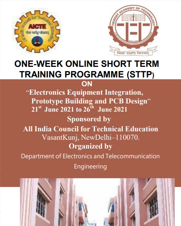
AICTE SPONSORED ONE-WEEK ONLINE SHORTTERM TRAINING PROGRAMME(STTP) ON “Electronics Equipment Integration, Prototype Building and PCB Design”

Post Views: 43,918 ABOUT THE STTP Department of Electronics and Telecommunication Engineering of Trident Academy of Technology, Bhubaneswar, Odisha, India is organizing AICTE sponsored, One Week Online Short Term Training Programme(STTP) on “Electronics Equipment Integration, Prototype Building and PCB Design” from 21st June to 26th June 2021. The third phase of the STTP scheduled from

AICTE SPONSORED ONE-WEEK ONLINE SHORTTERM TRAINING PROGRAMME(STTP) ON “Electronics Equipment Integration, Prototype Building and PCB Design” Read More »

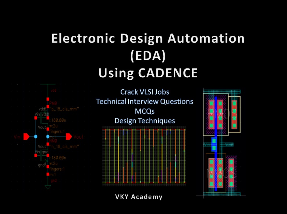
ELECTRONIC DESIGN AUTOMATION (EDA) USING CADENCE

Post Views: 2,875 TABLE OF CONTENT Introduction to CADENCE Use of CADENCE Cadence’s product offerings include Basic modeling using CADENCE Virtuoso Schematic Editor Virtuoso Analog Design Environment  Spectre AMS Designer Layout generation using CADENCE Introduction to low power IC design using CAD tools Need for Low Power Circuit Design  Low Power IC Design Using Cad

ELECTRONIC DESIGN AUTOMATION (EDA) USING CADENCE Read More »

The US Hits China With a Huge Microchip Bill FPGA Design Engineer Interview Questions Semiconductor Industry the huge break through