Welcome to your %Basic Electronics Quiz%
1. During reverse bias, a small current develops known as:
2. How does a semiconductor behave at absolute zero?
3. What are the charge carriers in semiconductors?
4. How are charge carriers produced in intrinsic semiconductors?
5. What type of material is obtained when an intrinsic semiconductor is doped with pentavalent impurity?
6. What type of material is obtained when an intrinsic semiconductor is doped with trivalent impurity?
7.In a PN junction the potential barrier is due to the charges on either side of the junction, these charges are
8. For a PN junction diode, the current in reverse bias maybe
9.When PN junction is in forward bias, by increasing the battery voltage
10. When a PN junction is reverse biased
12. A crystal diode has ………
13. The conductivity of a semiconductor increases with
14. The threshold voltage Vt of Silicon type PN junction diode is
15. The Knee voltage Vk of Silicon type PN junction diode is
16. The threshold voltage Vt of Germanium type PN junction diode is
17. The Knee voltage Vk of Germanium type PN junction diode is
18. A crystal diode has forward resistance of the order of ……………
19. The leakage current in a crystal diode is due to …………….
20.The knee voltage of a crystal diode is approximately equal to ………….
21. The disadvantages of a half-wave rectifier ……………….
22. The main disadvantage of a half-wave rectifier ……………….
23. The rectifier which always need a transformer ………………..
24. The PIV rating of each diode in a bridge rectifier is ……………… that of the equivalent centre-tap rectifier
25. For the same secondary voltage, the output voltage from a centre-tap rectifier is ………… than that of bridge rectifier
26. If the PIV rating of a diode is exceeded, ………………
27. The most widely used rectifier is ……………….
29. The ac resistance of a diode is
The identity factor n for GaAs is equal to

 JSPL Placement Papers
 GATE-2021 Syllabus vs GATE -2020 Syllabus for EC (Electronics and Communication)
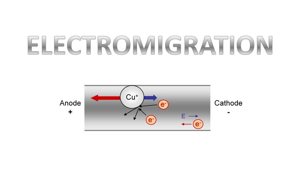 mechanisms in Integrated circuits
 PCB Design Job @ Inch Group, Gurgaon (Haryana)
 TCS CodeVita Season 9, 2020
 What is NDT (Nondestructive testing )?
 Electronics Engineering Huge Opportunities Ahead in the Field of VLSI and Chip Design
