


Part -1: Digital Fundamentals
1. How to design an AND gate using a 2×1 multiplexer?
To implement an AND gate using a 2×1 multiplexer (MUX), follow these steps:
- A 2×1 MUX has two data inputs (I₀ and I₁), one select line (S), and one output (Y).
- Let the inputs to the AND gate be A and B.
- Assign A as the select line (S = A).
- Connect I₀ = 0 and I₁ = B.
The output of the MUX becomes:
Y = A̅·0 + A·B = A·B
Hence, the MUX behaves like an AND gate.
2. Can a 2×1 multiplexer be considered as a universal circuit? If yes, how?
Yes, a 2×1 multiplexer is considered a universal circuit because it can be used to implement any logic gate or Boolean function by properly configuring its inputs and select lines. For example:
- NOT gate: Connect input to select line, I₀ = 1, I₁ = 0.
- OR gate: Use two 2×1 MUXes in combination.
- NAND, NOR, XOR, and XNOR can also be implemented using multiple 2×1 MUXes.
This flexibility makes the 2×1 MUX a universal building block in digital logic design.
3. What are the universal logic gates?
The universal logic gates are:
- NAND gate
- NOR gate
These gates are called universal because any Boolean function or logic circuit can be constructed using only NAND or only NOR gates.
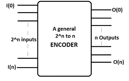
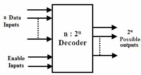
4. Explain the encoders and decoders with an example.
- Encoder: A digital circuit that converts 2ⁿ input lines into an n-bit binary code.
Example: An 8-to-3 encoder takes 8 inputs and produces a 3-bit output. If input D₅ is active, the output will be 101.
- Decoder: A circuit that performs the reverse operation of an encoder. It converts an n-bit input into 2ⁿ output lines.
Example: A 3-to-8 decoder takes a 3-bit input and activates one of the 8 outputs corresponding to the binary input.
5. What is the difference between Latch and Flipflop?
| Feature | Latch | Flip-Flop |
|---|---|---|
| Triggering | Level-triggered | Edge-triggered |
| Clock Dependency | Not required | Requires clock |
| Speed | Faster | Slower |
| Usage | Simple memory storage | Synchronous systems |
| Example | SR Latch, D Latch | D Flip-Flop, JK Flip-Flop |
In short, latches are simpler and respond to input changes continuously, while flip-flops respond only at clock edges.
6. What is setup time and hold time?
- Setup Time: The minimum time before the clock edge during which the data input must remain stable to be correctly latched.
- Hold Time: The minimum time after the clock edge during which the data input must remain stable.
Violating these constraints can lead to incorrect data being stored or metastability in flip-flops.
7. What is FSM? What are the types? Which one is preferred?
- FSM (Finite State Machine) is a model of computation used to design sequential logic circuits. It consists of a finite number of states, transitions, inputs, and outputs.
Types of FSM:
- Mealy Machine – Output depends on current state and input.
- Moore Machine – Output depends only on the current state.
Preferred Type:
- Moore machines are generally preferred for their simplicity and predictable output behavior, especially in synchronous systems. However, Mealy machines can be more efficient in terms of state count.
Part -1: Verilog
Related posts:
 Full VLSI Flow for a 2-bit Adder with DFT Verification
 Design Verification Interview Question with Answer-Part-1
Solutions of FPGA Design Engineer Interview Question Part-1
DFT Verification Interview Questions with answers Part-1
Design Verification Interview Question with Answer-Part-1
Solutions of FPGA Design Engineer Interview Question Part-1
DFT Verification Interview Questions with answers Part-1
 TCS CodeVita Season 9, 2020
 Graduate Aptitude Test in Engineering (GATE) 2020
 GATE-2021 Syllabus vs GATE -2020 Syllabus for EC (Electronics and Communication)
 Introduction to Boolean Algebra and Fundamentals of Logic Gates